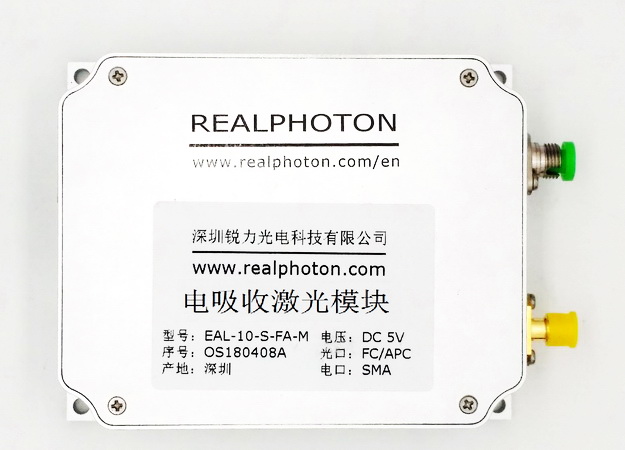

双光纤尾纤输入,速率43Gbps, 可应用于DPSK系统; 射频接口GPPO, 差分输出; 差分转换增益2600V/W,3dB截止频率35GHz.
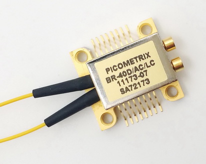
40Gbps, PICOMETRIX Balanced Photo-receiver, BR-40D, CL Band
Descriptions
The balanced receiver module is ideally suited for a variety of applications up to 43 Gbps such as D/BPSK, D/QPSK and . The module consists of a pair of balanced photodiodes and a high-gain limiting transimpedance amplifier. The module has a typical conversion gain of 2400 V/W. Its dynamic signal integrity control allows excellent OSNR performance , which result in optimum eye pattern and the minimum bit errors ratio. The module is available with differential GPPO RF outputs , AC coupled options.
Applications
- 43Gbps DPSK, QPSK Optical Transceiver
- Radio Over Fiber, and Fiber Sensing
- Testing and Measurement
Features
- Sensitivity, -10dBm typical, C&L Band
- Typical 35GHz 3dB cut-off frequency
- 550mVpp differential output voltage
Optical Characteristics
| Parameter | Units | Min | Typ. | Max | Notes |
| Wavelength Range | nm | 1200 | 1650 | Usable range | |
| Bit Rate | Gb/s | 43 | NRZ format | ||
| PD Responsivity | A/W | 0.55 | 0.65 | 0.75 | Avg. polarization at 1550nm |
| Conversion Gain(differential) | V/W | 2200 | 2600 | 3000 | CG=diff. output swing/total input swing @-10dBm NRZ input,Vc=-3.2V |
| OSNR Sensitivity* | dB | 13 | OBW=0.1nm,Vc=optimized,DPSK system with BER le-3* | ||
| Max. Operating Input | dBm | +6 | Into each photodiode (average level,NRZ) | ||
| Limiting Level Input | dBm | -10 | NRZ, approximate;ER>10dB.Above this level of modulation input the electrical output swing is limiting | ||
| Optical Input Return Loss(ORL) | dB | <-30 | -27 | ||
| Polarization Dependent Responsivity(PDR) | dB | 0.12 | 0.2 |
Note: * over operating case temperature specification at 1310nm and 1550nm; ** This is a DPSK system level test. Results depend heavily on other equipment used in system level testing;the typical value assumes system-level optimization which takes into account the electrical backend which receives the output signal form the BR-40 module(i.e. the DeMux and/or clock-data recovery component involved in BER results);
Electrical Characteristics
| Parameter | Units | Min | Typ. | Max | Motes |
| Large Signal Bandwidth (-3dB) | GHz | 32 | 35 | Large signal tested at 3dBm avg,25% modulation at this level;single-ended testing each input | |
| Electrical Return Loss | dB | -10 -8 | 0.1-25GHz 25-35GHz | ||
| Max. Output Swing | mV | 450 | 550 | 650 | Differential |
| AC Coupling Cutoff Frequency | KHz | 100 | For AC coupled options only;>-3dB for frequencies below this | ||
| DC Output Pickoff Offsets(DC) | mV | -250 | -200 | -150 | With RF outputs DC-coupled to 50ohms terminated to ground,levels equalized. |
| DC Output Pickoff Offset Resistance | ohms | 5k | (internal pick-off resistor value) | ||
| Rise/Fall times | ps | 10 | Measured with>50GHz sampling oscilloscope and risetime of sampler deconvolved from result | ||
| Timing Skew | ps | 1 | 2 | Average group delay difference of all four input/output signal paths(avg.4-20GHz) | |
| Photodiode Dark Current | nA | <5 | 10 | At 25℃ | |
| Photodiode Bias Decoupling Capacitance | nF | 10 | Internal decoupling capacitance on each PD bias pins | ||
| DC Input Offset Voltage Range | V | -9 | 9 | Voltage over this range can be applied to correct for unbalanced avg optical input powers | |
| DC Input Offset Impedance | ohms | 3000 | Input resistance in series internally with each DC Input offset | ||
| Control Input Voltage Range | V | -5 | -2.5 | 0 | 3mA max at limits |
| Maximum Control Input Current | mA | 3 | Maximum current at Control Input Voltage min/max | ||
| Control Voltage Input DC Level(open) | V | -3.25 | -3.2 | -3.15 | |
| Output Coupling | AC | DC is optional upon request (determined by specific part#) |
Note: * over operating case temperature specification;
Block Diagram